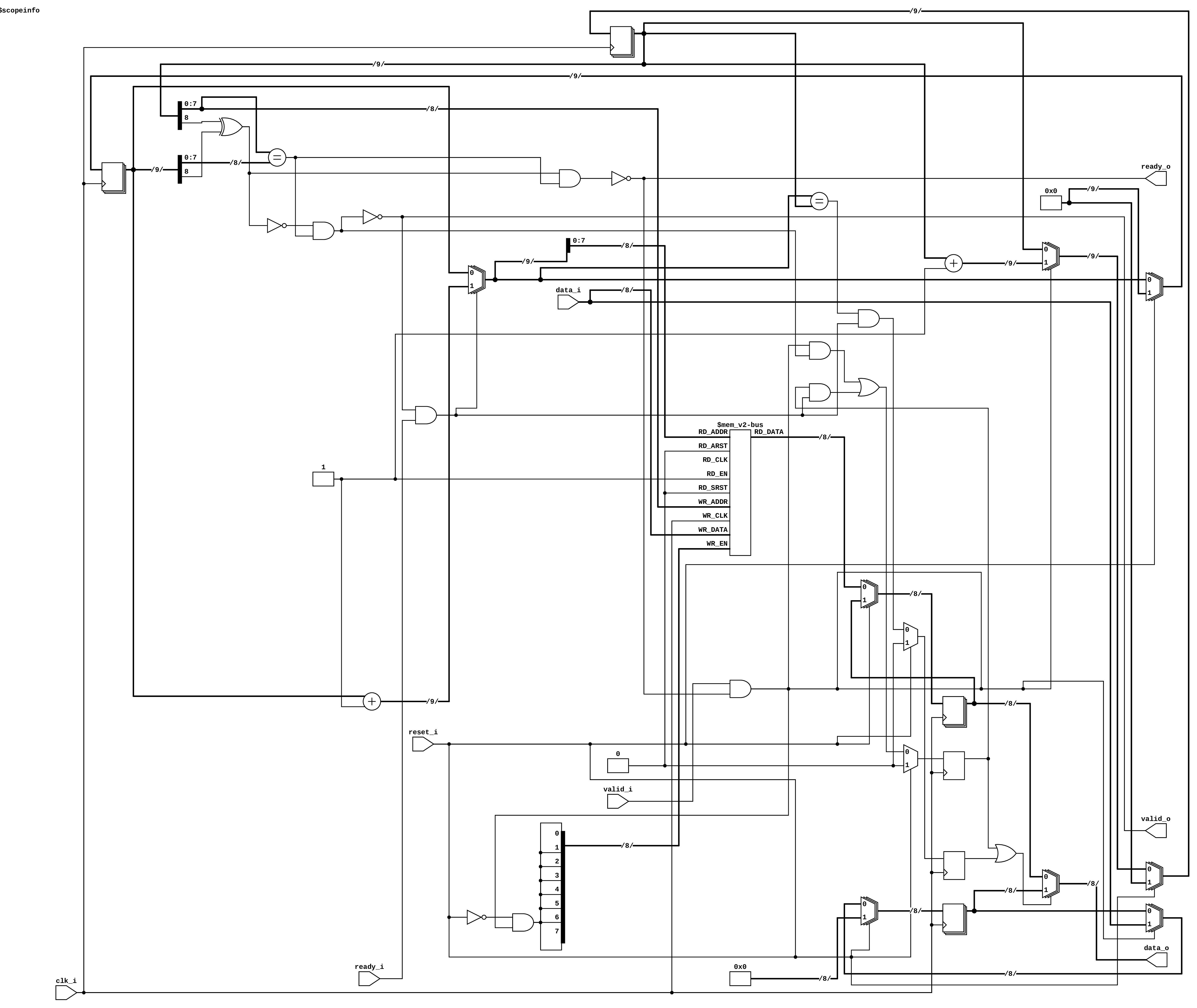
Synchronous FIFO Design

Synchronous FIFO Design
Description:
In this lab, I designed and implemented a parameterized 1R1W (one-read, one-write) synchronous memory module in SystemVerilog, emphasizing read-priority operation and FPGA synthesis compatibility. After verifying correct functionality through simulation, I used Yosys to confirm that the design was properly recognized as an FPGA block memory. Building upon this, I developed a synchronous FIFO module using my custom RAM component, addressing timing challenges introduced by synchronous reads. I optimized the design by incorporating hazard-style data forwarding to reduce read latency and achieve full functional performance. Finally, I demonstrated the FIFO in a real-time hardware application by buffering audio signals between the input and output interfaces of an FPGA board, showcasing efficient synchronous memory operation in a practical system.