LUT Logic Design
LUT Logic Design
Description:
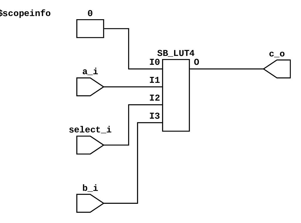
In this lab, I explored how FPGA logic is synthesized at the hardware primitive level by implementing digital circuits directly using look-up tables (LUTs) and other low-level FPGA resources. Instead of describing logic behaviorally or structurally as in previous labs, I instantiated vendor-specific primitives such as Xilinx LUT6, Lattice ICESTORM_LC, and SRL16E modules to recreate standard logic functions. I implemented 2-input XOR, XNOR, and MUX modules by defining the proper LUT initialization patterns (LUT_INIT), manually encoding truth tables into the corresponding bit strings. I then created a full adder using either dual LUT6 modules or the ICESTORM_LC primitive by configuring its internal carry chain logic through parameters like CARRY_ENABLE and CIN_SET. To further optimize multi-operand addition, I designed a triadder module using a 3:2 compressor approach to efficiently sum three inputs while minimizing propagation delay. Finally, I implemented a delay buffer using the SRL16E shift-register primitive, which stored and released input data after a configurable number of clock cycles. This lab gave me practical experience in manual logic synthesis, deepened my understanding of FPGA architecture, and reinforced how EDA tools map high-level HDL code into low-level hardware resources.