Delay Buffer Design
Delay Buffer Design
Description:
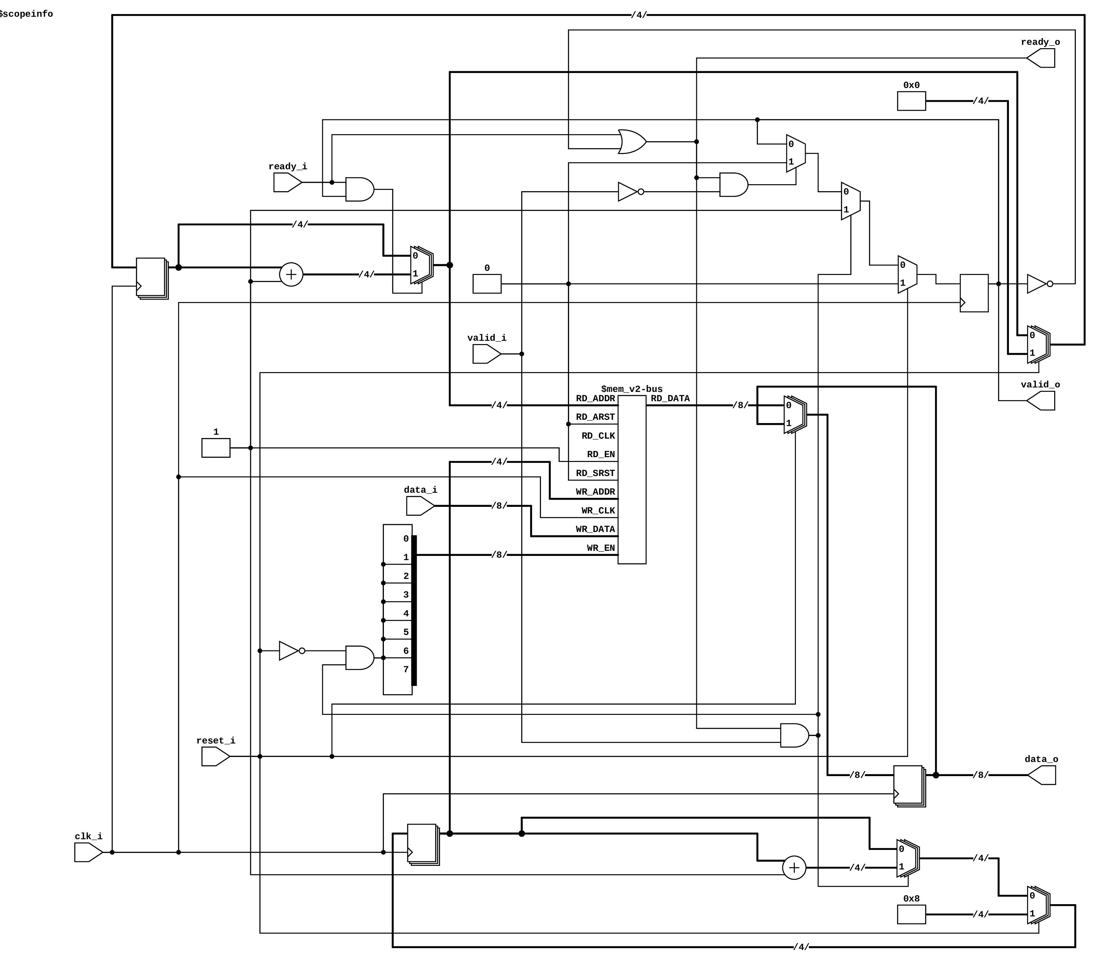
In this lab, I designed and implemented multiple types of delay buffers in SystemVerilog to explore timing control and data flow management in FPGA-based systems. I first developed a register-based delay buffer that introduced a fixed number of ready/valid handshakes between input and output data, demonstrating parameterized delay and width functionality. I then created a counter-roll module to support address wrapping, which was integrated into a RAM-based delay buffer built using my previously designed synchronous memory (ram_1r1w_sync). This design used FPGA block RAM to efficiently store and retrieve delayed data with constant latency determined by the delay parameter. After verifying functionality through simulation, I generated post-synthesis schematics in Yosys to compare FPGA resource utilization between register-based and RAM-based implementations, analyzing trade-offs in compilation time, area efficiency, and synthesis behavior.